
MicroLED Test and Transfer Solution
✹ MicroLED Probing and Testing System ✹ MicroLED Laser Lift-off System ✹ MicroLED Laser Transfer System ✹ MicroLED Laser Bad Dies Dumping System ✹ MicroLED Optical Inspection System ✹ MicroLED Laser Implant System |
MicroLED Test and Transfer Solution
FitTech has comprehensive MicroLED test and transfer solution, provides coustomized equipment specifications and equipment recommendations based on different requirements for wafer fabrication or panel industry.
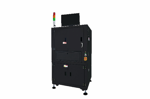
Process equipment
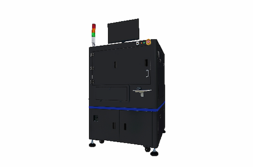
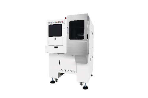
MicroLED Probing and Testing System
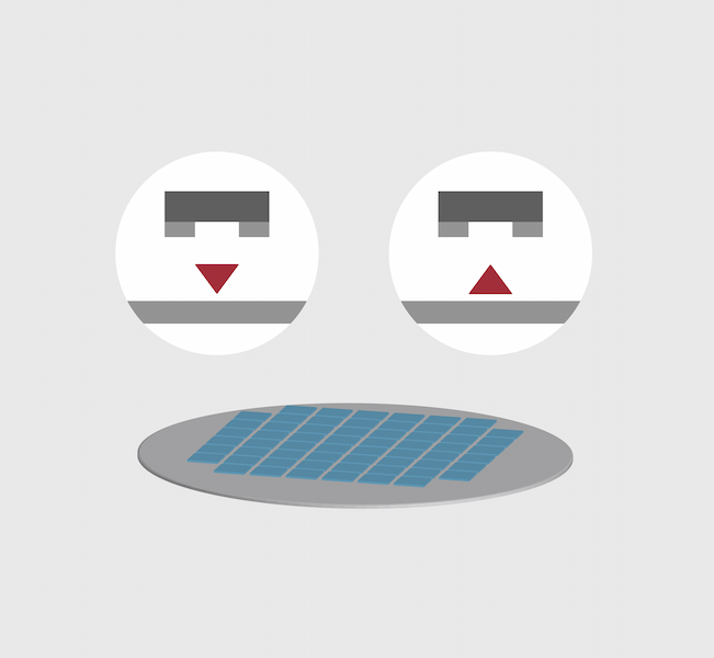
Testing the brightness, wavelength and driving voltage of µLED on COW/COT or MIP µLEDs
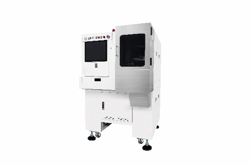
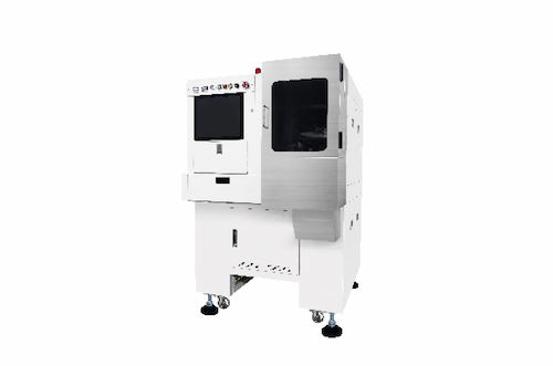
MicroLED Laser Lift-off System
Transferring the entire epitaxial layer on the epitaxial substrate to another substrate or carrier
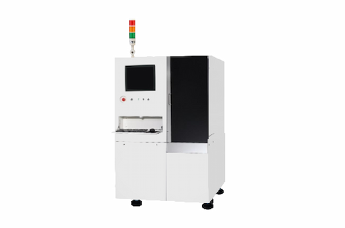
MicroLED Laser Transfer System
Transferring µLED chips from the original substrate or carrier to a new substrate or carrier
MicroLED Laser Bad Dies Dumping System
Remove the NG chips / bad dies from the substrate or carrier
MicroLED Optical Inspection System
Recording the NG chip from substrate or carrier via image recognition
MicroLED Laser Implant System
Transfer new chips to the missing crystal position on the missing crystal substrate or carrier
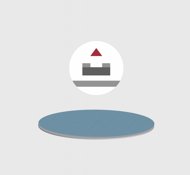
Substrate definition and transfer purpose
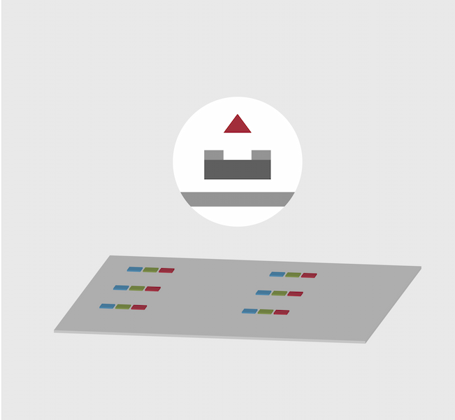
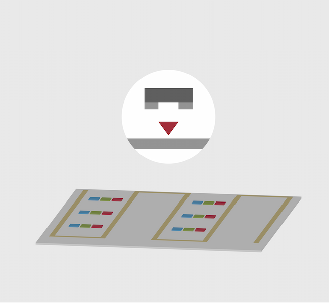
■ Chip flipping (electrode facing up or down)
■ Transfer µLED chips to another substrate (equidistant or Enlarged equidistant)
μCOW
(μChip on Wafer)
μCOC
(μChip on Carrier)
μCOT
(μChip on Template)
μCOB
(μChip on Backplane)
For more detailed equipment specifications or further requirements, please feel free to contact us.